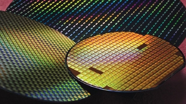
TSMC 7nm UEV design has been finalized and although we already know about 7nm chips that are in the works, these are different. These are second generation TSMC 7nm chips that will use extreme ultraviolet lithography for four non-critical layers. This will enable faster production.
We do not know much regarding the difference between the 7nm and the 7nm+ process but what we can tell you is that the new process (TSMC 7nm UEV design) will offer a 20% higher transistor density. It will also offer 8% lower power consumption and higher frequency as well.
AMD chips are going to be based on the 7nm process and the AMD Vega graphics cards are going to be based on the same node as well. AMD Navi will be based on the 7nm+ process so we should learn about the difference in performance. TSMC has not revealed for whom this design has been finalized but it is a matter of time before this becomes common knowledge.
After the TSMC 7nm UEV design, the fab is going to work on the 5nm process. This should be a significant leap. As compared to the 7nm process the 5nm process should consume 20% less power. It will also offer 15% better performance and the area will be reduced by 45%.
AMD has confirmed that CEO Lisa Su will talk about 7nm chips at CES 2019. So that is something to look forward to. According to the company:
In 2019, AMD will catapult computing, gaming, and visualization technologies forward with the world’s first 7nm high-performance CPUs and GPUs, providing the power required to reach technology’s next horizon.
We also got some benchmarks concerning the upcoming 7nm Vega GPUs and according to the numbers, the upcoming graphics cards are up to 65% faster as compared to the AMD RX Vega 64. That is a very impressive increase in performance.
Let us know what you think about the TSMC 7nm UEV design and whether or not you are interested in buying CPUs that are based on this new technology.
